How Do Beamsplitters Work?
Flatness of Beam Splitters
Microscopes and optical setups in general consist of various optical components, and the performance of the system (resolution, contrast, etc.) can be negatively affected due to wavefront errors.
Wavefront errors always occur as soon as the surface of an optical component deviates from its respective ideal shape. To describe the wavefront error, one assumes a plane wavefront (surface with the same phase of the wave), which usually moves orthogonally to the propagation direction. This wavefront is deformed due to the non-ideal surface of optical components. Two types are distinguished:
- Reflected Wavefront Error (RWE),
- Transmitted Wavefront Error (TWE)
With more and more high-resolution microscopy methods such as TIRF, STED, etc., the reduction of the wavefront error in the system plays a decisive role. Therefore, when selecting an optical filter or beam splitter, the flatness of the optical component should be specified and selected according to the application so as not to affect the performance of the system.
Reflected Wavefront Error of Beam Splitters (RWE)
In the case of reflected wavefront error (RWE), the wavefront reflected from a surface and the resulting error are considered. The curvature (convex, concave) and the unevenness of the beam splitter primarily have a negative effect on the reflected wavefront. The beam reflected by 180° gets a deviation twice as large as the distance of the surface error (flatness) of the beam splitter due to the double path. For reflections not equal to 180°, the reflected wavefront error is multiplied by the cosine of the angle of incidence to the normal of the surface:
RWE = 2 * Flatness * cos(AOI)
To illustrate the effect of a non-planar beam splitter, we consider the reflection of a laser from a curved (A) or flat (B) beam splitter and the image produced on the wall or ceiling.


Image 1: © Semrock Optical Filters – IDEX Health & Science
Image 2: © Semrock Optical Filters – IDEX Health & Science
Transmitted Wavefront Error of Beam Splitters (TWE)
Transmitted wavefront error (TWE) considers the non-ideal wavefront after passing through an optical medium (lens, beam splitter, optical filter, etc.), where the error is the sum of the errors of both surfaces (front and back). The total wavefront error can be divided into a wedge error (non-parallel surfaces), a spherical, curved component (concave / convex lens) and a diffuse, non-regular component. As a rule, the wavefront error generated by transmission is relatively small and can be neglected.
How to Specify the Flatness of Beam Splitters?
Unfortunately, the specification of the flatness of beam splitters is not uniform, which is why you have to look carefully when comparing the flatness of different manufacturers. In general, however, the deviation or error is specified in units of a reference wavelength (632.8 nm in the ANSI standard and 546.07 nm in the ISO standard) over a defined area (usually a circular area with diameter 1 inch = 25.4 mm).
PV or Peak-to-Valley
In peak-to-valley (PV, mountain to valley), the specification of unevenness refers to the difference of the highest to the lowest point within a defined area (1 inch or the free aperture). Consideration must also be given to what exactly is being specified: the unevenness of the object or the reflected/transmitted wavefront. The reflected wavefront error is up to twice the unevenness of the reflecting surface and depends on the angle of incidence. The transmitted wavefront error is made up of the front and back - where it can be smaller than the sum of the individual errors of a surface.
RMS
RMS or rms means "Root Mean Square". In a simple form (only "positive" deviations, as in a "salad bowl"), the RMS value is approximately 70% of the "PV" value. For an irregular deviation, like a "potato chip," this value drops to about 30%. If the surface defect is more like a lunar surface, consider the many different irregularities separately, square them each, add them together, divide by the number of irregularities, and finally take the square root of them (the alternative representation expresses it a bit more elegantly, t equals x here):

The RMS value is more suitable if the surface defect is composed of different or very punctual unevennesses and is not uniform. For the roughness of a surface, the RMS is therefore more suitable. To describe the "deformation" of a non-flat (but possibly smooth) surface, the PV value or radius of curvature is more suitable.
Thought experiment: What to do if you only have a deep, small hole in one place (e.g. pinhole)?
The advantage of the RMS value is: it tries to capture the unevenness as a whole. The disadvantage is: it is not so easy to determine and less descriptive or understandable.
Radius of curvature
Mathematically, the curvature (κ) indicates the local deviation from a straight line and is inversely proportional to the radius (R):
R = 1 / κ
Due to the (reasonably symmetrical) curvature of the beam splitter, a focus is created so that a collimated beam has a focal point. The distance to the focal point corresponds to half the radius of curvature of the surface. (Approximation: spherical mirror, rays close to the axis).
Manufacturing Flat Beam Splitters
Wavefront defects arise, on the one hand, from the stresses due to coating from the many layers of different material and thickness and, on the other hand, from coating irregularities or "passed on" substrate surface defects. The first defect creates a curvature like a kind of parabolic mirror ("salad bowl") and the other defect a kind of lunar surface.

To show the relationships, we consider the stress generated by the coating that causes the curvature (δ in µm), the diameter (free aperture) of the surface under consideration (D in mm), the coating thickness (f in µm, where the difference is considered for double-sided coatings), the substrate thickness (s in mm), and a dimensionless constant C (depending on the glass type, coating material, etc.):
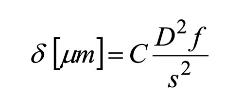
This shows that the flatness is quadratically related to the substrate thickness and the area under consideration – and linearly related to the coating thickness. This means that it is first necessary to check whether the required flatness can be achieved by a smaller aperture or a thicker substrate. If not, the coating thickness can be effectively reduced by spreading the coating over the front and back surfaces, although this will drive up the cost due to the longer coating time. Alternatively, the coating thickness can be reduced by a simpler design – but at the cost of spectral performance (steepness of edges, blocking, etc.).
Image 4: © Alluxa
Thick substrate
The next obvious step to reduce wavefront error is to use thicker substrates (as in making mirrors), e.g., 3 mm or even 5 mm thick substrates. This helps – but has the catch that the beamsplitters need special holders and have a larger offset of the transmitted beam that must be taken into account.
Backside countercoating
Another common way to compensate for stresses is to split the coating in two and coat the beamsplitter front and back. This creates a counter stress and the beam splitter is flatter in total than if the whole coating was on one side. However, one has to be careful here, because due to the second coating on the back, spectral components are reflected on the back and can lead to a "ghost effect". In reality, this results in more or less intense double images. If it is used selectively and the two spectra from the front and back side are known, this technique can be used without any disadvantages.
Special coating processes
With special coating equipment it is possible to reduce the surface tensions as far as possible and to produce very flat beam splitters with a standard thickness of 1 mm. However, with the framework condition of flatness, not any number of layers can be applied, so the spectral edge between reflection and transmission cannot be arbitrarily steep. This means that the beam splitters are not suitable for all applications, since in some cases the useful signal is spectrally very close to the excitation (e.g. Raman).
Mounting of flat beamsplitters
Producing and measuring super-flat beam splitters is one thing – mounting them in such a way that the flatness is still guaranteed at the end is another. If unfavorable mounting stresses act on the beam splitter when it is installed in a filter cube due to bonding or clamping, this can deform the beam splitter and, in the worst case, make it unsuitable for the application. This is especially true for high-resolution microscopy techniques such as TIRF, STORM, PALM, GDSIM, STED, MINFLUX, etc.
If you would like to benefit from our many years of experience in this regard, we would be happy to take care of the filter assembly for you:
Applications and Specifications of Beam Splitters
| Application | Substrate Thickness (mm) |
Curvature Radius (m) |
Reflected Wavefront Error (RWE) at 632.8 nm, PV |
Max. Beam Biameter (mm) – not imageable |
Max. Beam Diameter (mm) – imaged |
|---|---|---|---|---|---|
| STED, TIRF, PALM, STORM | 3 | ~ 1275 | < 0.2 λ | 22.5 | 37.0 |
| dito | 1 | ~ 255 | < 1 λ | 10.0 | 16.7 |
| Imaging reflection (Image Splitter) |
3 | ~ 1275 | < 0.2 λ | 22.5 | 37.0 |
| dito | 1 | ~ 100 | < 2 λ | 6.3 | 10.0 |
| Laser (confocal, multiphoton) | 1 | ~ 30 | < 6 λ | 2.5 | 6.0 |
| Standard Epi fluorescence | 1 | ~ 6 | >> 6 λ | NA | NA |
| Source: Semrock Optical Filters – IDEX Health & Science | |||||
The table gives an orientation which flatness is required for a beam splitter depending on the application. Experience has shown that the use of beam splitters with a smaller PV or radius of curvature specification is advisable for STED microscopy and general confocal microscopy.
In practice, 5 or 6 mm thick beam splitters are used in STED microscopy. It is noticeable that the possible free aperture or maximum beam diameter for non-imaging beams is smaller than for imaging beams. This appears counterintuitive at first, since imaging beams additionally contain the location information of the sample, in contrast to non-imaging beams. The reason for this can be found in the different limiting criteria. The non-imaging beams are based on the Rayleigh length criterion (see below) and the imaging beams are based on the Airy Disk / Rayleigh criterion.
Non-imaging Beams
Non-imaging beams primarily contain the spectral information and the respective intensity (time could still be included, but is not often the case). The sample is rastered and the image is assembled afterwards in the computer using a lot of point information. This is e.g. the case in the confocal microscope (LSM) and in the STED microscope. The Rayleigh length criterion states that the focus offset must be less than one Rayleigh length due to the reflected wavefront error. Not to be confused with the Rayleigh criterion that separates two image points (see imaging beams). It should be noted that the Rayleigh length decreases with larger beam diameter (or NA).
If one now plots the beam diameter against the maximum wavefront error (or the minimum flatness, which is proportional to it), the following diagram results:


Image 5: © Semrock Optical Filters – IDEX Health & Science
Image 6: © Semrock Optical Filters – IDEX Health & Science
Image Forming Beams
Imaging beams contain the information of non-imaging beams, plus the location information (x/y axis) of each point (image). The decisive factor here is the point at which two points can be perceived as separate (resolving power). The Rayleigh criterion considers two diffraction discs/images (airy discs) with the same color and brightness and their diffraction rings. The resolving power then corresponds to the distance of the two diffraction images of 0th order, which just do not overlap any more (Source: University of Vienna, "Light microscopy online")
The resolving power can also be colloquially compared to image sharpness. The following diagram shows the influence of the flatness of a beam splitter (radius of curvature m) on the image sharpness:

Image 7: © Semrock Optical Filters – IDEX Health & Science
The Airy Disk / Rayleigh criterion states that the magnification of the beam diameter due to the reflected wavefront error must not be greater than 1.5 times the Airy Disk diameter. For a concave/convex curved beam splitter, the maximum imaging beam diameter depends on the wavefront error (PV/inch) or flatness. This results in the following diagram, from which the maximum wavefront error (PV/inch, and from this the flatness) can also be derived depending on the own beam diameter.
Applications of Beam Splitters
Beam Splitters for Epi Fluorescence Microscopy
In classical epi-fluorescence microscopy, the non-coherent excitation light is reflected onto the sample via the beam splitter and the fluorescence image is transmitted through the beam splitter. The resulting deviations from the beam splitter can usually be neglected, since the spot size and depth of excitation are not critical and the sample is excited over a wide area. The influence of the transmitted wavefront error on the fluorescence image is usually also marginal and not relevant.
Conclusion: Standard beamsplitters can be used without compromising the quality of the application.
Beam Splitters for TIRF Microscopy
In TIRF (Total Internal Reflection Fluorescence) microscopy, the evanescent field of a totally reflected excitation beam (usually laser) is used to excite the sample in a very limited (exponentially decreasing) region behind the boundary layer (100–200 nm). This strongly limits the area that can fluoresce and thus obtains selective image information. Deviations from the ideal beam path can lead to the excitation light no longer being totally reflected, but also penetrating the sample. Since the evanescent field decreases exponentially and the total reflection depends on the angle, the method is very error-prone (see picture: laser on the wall). For more information, see our article about » TIRF microscopy.
Conclusion: Very flat beam splitters must be used to minimize the wavefront error.
Beam Splitters for STED Microscopy
STED stands for "Stimulated Emission Depletion" and is a method in fluorescence microscopy in which the diffraction limit is bypassed and thus an image resolution of less than 40 nm is possible. For imaging, the sample is scanned, as in a confocal microscope, and the image is subsequently stitched together from the pixels. The trick is that in addition to the scanning laser (to excite the fluorescent dye), a second laser is used, which has the shape of a "donut" (ring with a hole in the center) and is focused on the same spot. The "donut" with the fluorescence wavelength now ensures that the fluorophores in the sample are "excited" (returned to their ground state) and can no longer fluoresce. What remains are the fluorophores in the center of the "donut" ring, whose fluorescence intensity is measured and used for imaging.
Conclusion: Since the shape of the excitation point and the "donut" are elementary, it is fundamentally important to use planar beam splitters.
Sources:
- Maximizing the Performance of Advanced Microscopes by Controlling Wavefront Error Using Optical Filters (PDF),
by Semrock Optical Filters – IDEX Health & Science - Surface Flatness and Wavefront Error, by Alluxa